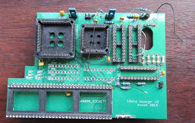
The final V2 booster design as listed above had a great many prototypes before it reached a working versions which I was happy with (as shown above). I thought I would just post 2 of the early prototypes as I found them in my drawer, while looking for something else.
It's not very hard to see whats going on above. Classic 68000 CPU there. Plus 2 1MB ROM's. This board suffered badly from various faults and grounding issues and moved to a new design later.
The next version moved to a PLCC ROM and PLCC 68000 CPU. Though sadly this board ended up being produced twice due to a broken 0v polygon :(
In fact while the bottom of the CPU was actually connected to 0v, the broken polygon caused a bad 0v path and caused a spike between 0v pins on the CPU.. (This actually is one problem with DMA issues on the STE with the CPU)
This was causing signals on the GAL to reach 7volts! Things went horridly wrong with that layout :( So another batch of PCBs was junked.
It was at that point I decided to move to 4 layer boards. mostly 2 layers for signals, and a dedicated layer for 5V and 0V. Going by each PCB designed had some issue relaying to spikes in 0V paths etc I think it was time to forget 2 layer boards and just move onto something rock solid.
In the end the V2 booster ended up on a 6 layer board, and the development costs, and indeed production costs went though the roof on the V2 booster :(
At the time of typing there is only a couple V2 booster left and it is unlikely there will be produced again. There never seems to be a high demand for boosters, and I can't do them any cheaper without doing larger batches, which I doubt would sell.
While this booster has TOS104 and TOS206 onboard, it also has a 16MHz boost with 16MHz access to ROM. This gave the booster a good kick in speed in desktop apps which used TOS a lot.
Its very similar to the V1.5 booster for the STFM. Similar idea, just without TOS206 built on. I did think as the V2 was large, it only fitted one style of motherboard. Aside from the MEGA ST. It was one reason I produced the V1.5 booster. Though sadly, that seemed less popular than the V2 :( The V1.5 booster could be fitted to probably any machine as well.
I have been working on 32MHz boosters for the STFM. Though I think that work will be suspended, maybe indefinitely as most people seem to want boosters for the STE lately.
If there is interest, I may sell a couple of motherboards fitted out with the V1.5 booster. I know there need a lot of soldering, so possible that is the main reason people are put off buying such things as they do need a lot of soldering. Though it is unavoidable unfortunately.
My past booster work can be found here.
V2 booster webpage
V1.5 booster webpage
Web Store


Love seeing prototype pics of stuff :)
ReplyDeleteDo you have a collection of boards that went wrong or never made it to production, the story behind the attempts are interesting.
Those green ones "went wrong". Though everything which didn't make it to production either went wrong or never got finished.
DeleteIts just how things are. Design something as best you can. Then iron out all the bugs, do a second PCB, then find more bugs and iron them out.. Normally each project I do will have 3 or 4 versions of the same thing which didn't work as expected.
When it can cost £50-£200 for a run of PCBs. Mostly they just end up getting binned as just can't use them :( Then I have to factor that "loss" of money into the final selling price of the kit.
Even the final V2 booster had 2 "mistakes" on it. I had trouble with the GAL as some pins could only have 10 "gates" on it. I needed 11 for one pin. So its why the GAL on the right basically has 2 pins swapped because at the time I didn't know about the limitations on various pins. Of course 6 layer boards costing like £30 each and 25 of them.. I couldn't really scrap those boards.
I think there was several versions of that booster which was built. I have many more design variations of it in my PCB software as well.
I guess it can be like 20 designs, where 7 got real PCB's made and 1 made it into a production kit. I have to keep tabs on all these PCB costs.. its just become a nightmare.
Its why I think its just time to move onto a new motherboard and have done with a lot of problems. Its just become tiresome to design something, then spend months trying to work out why it doesn't work because of some noise on some signal on the motherboard. Not only that, but I'm getting rather bored of spending endless hours doing PCB designs.